Advancing the Future of Optics Through Planar and Metalens Engineering

MetaRosetta
Traditional Lenses

Innovating Beyond
Traditional Lenses

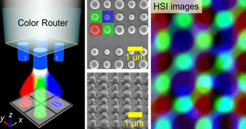
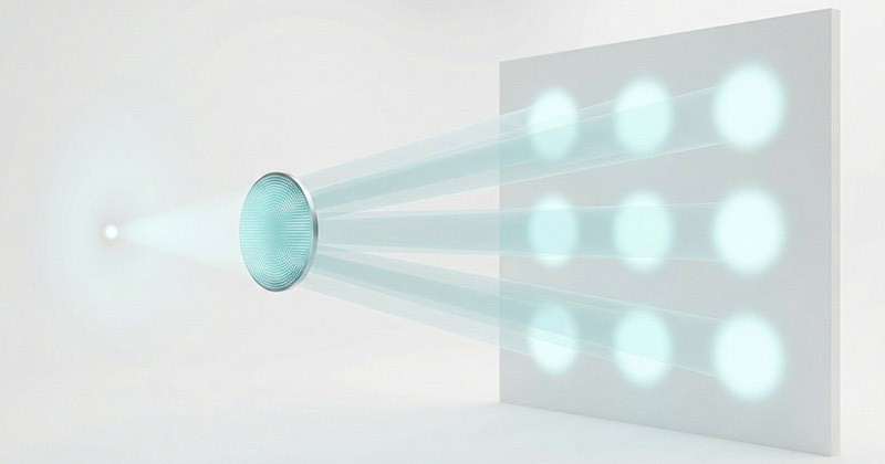
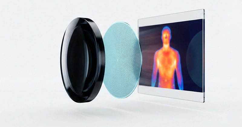
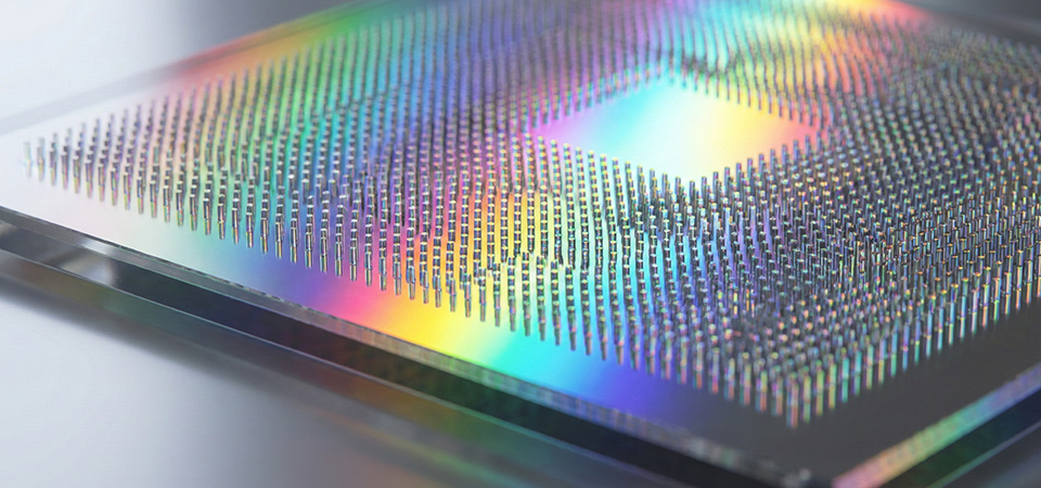
MetaRosetta is an innovative company developing advanced metalens with nano-level precision using semiconductor processes. We offer design services and product integration to enhance clients' products through metalens technology.

Our solutions have broad applications in automotive thermal imaging, industrial inspection, medical diagnostics, and smart technologies such as Face ID.

  • Visible (450-750 nm)

    Visible (450-750 nm)

    As CIS pixel sizes continue to shrink, the goal is to achieve higher spatial resolution, smaller device size, and lower cost. However, reducing pixel size decreases the light-receiving area of each pixel, directly leading to a decline in optical sensitivity. Additionally, traditional dye-based color filters, which are about 200 nm thick, occupy space in miniaturized pixels and limit the flexibility of optical design.
  • NIR (850-1550 nm)

    NIR (850-1550 nm)

    Traditional optical components have become the size and weight bottlenecks for the next generation of ultra-compact NIR sensing modules.
  • LWIR (8-12μm)

    LWIR (8-12μm)

    As optical sensing modules continue to shrink, achieving high sensitivity within limited pixel areas becomes increasingly challenging. Our metasurface-based Metalens technology replaces traditional multi-element optics with nanoscale structures, enabling compact designs while maintaining high optical efficiency and precision.
  • Customization

    Customization

    Meta Rosetta is our proprietary nanophotonic design platform built to unlock the full potential of Metalens technology. By combining advanced computational optics with process-aware design, it enables highly efficient, ultra-compact, and manufacturable metalens solutions for next-generation optical systems.
Latest News
  • Dec26

    AWARDS

    Awards

  • Dec16

    MEDIA COVERAGE

    Eight startups from the Hsinchu Science Park showcased cutting-edge technologies at Singapore Technology & Innovation Week.

  • Dec09

    MEDIA COVERAGE

    Taoyuan Youth Innovation Expo gathers international resources and aims to become a landmark innovation hub in the Asia-Pacific r

  • Dec08

    MEDIA COVERAGE

    Chuo University's advanced optics capabilities have been recognized by authoritative Japanese media.

  • Dec08

    MEDIA COVERAGE

    National Central University's innovative company, Keyingda, has taken its technology to the international stage with its adv

  • Nov25

    MEDIA COVERAGE

    Beyond Taiwan's new creative endeavors: Why is Portugal a crossroads for entering the international market?

  • Nov13

    MEDIA COVERAGE

    Taiwanese startup designs metalens, targeting US automotive infrared cameras.

  • Oct29

    MEDIA COVERAGE

    Exploration Southeast Asia Market Edition 8 Outstanding New Founding Groups of Bamboo Shooting Teams Shinkapo SWITCH Exhibition

  • PRODUCT

  • TECHNOLOGY