
The Invisible "Optical Revolution": How Startup Ingenics Breaks Through the Physical Limits of Traditional Optics Using
2026.04.24
Article quoted from:https://meet.bnext.com.tw/articles/view/53183?
The thickness of modern mobile phones is partly limited by the size of their lenses. With Apple and Samsung incorporating "super lenses" into their next-generation product plans, we can perhaps begin to anticipate even thinner and more stylish phones in the future. Going further, perhaps we'll be able to wear VR devices as thin as glasses and see adorable creatures carrying fruit, causing flowers to bloom wherever they go.
This is precisely the future that the startup Techtronic Industries is striving to accelerate. Leveraging its extensive experience in the semiconductor industry and its knowledge of optics, the team is working hard to overcome material and process limitations in "super-lenses," which have long remained in laboratory research, transforming them from expensive experimental products into products that can be mass-produced and used in everyday life.
What is a superlens? Where can it be used?
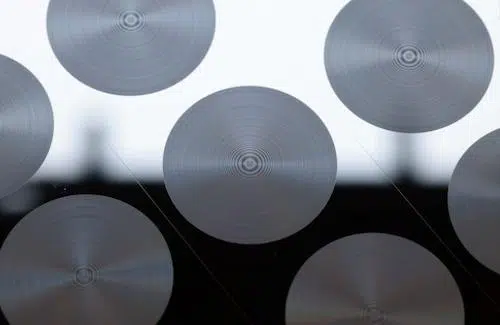
Metalens are not traditional curved lenses made of ground glass, but rather extremely thin "planar" optical elements that need to be manufactured using semiconductor processes.
Its surface is covered with tens of millions of nanopillar structures smaller than the wavelength of light. These structures act like a precisely choreographed optical control system,
which can change the direction and speed of light as it enters, thus performing the refraction function of a traditional lens to achieve a focused imaging effect.
The biggest advantage of this technology lies in its thinness and lightness. Superlenses have the potential to replace the stack of up to six or seven lenses typically found on the back of a smartphone camera with a single thin film, significantly reducing its size and weight. This not only opens up more design possibilities but also becomes a key technology for improving the wearing comfort of wearable devices (such as AR and VR).
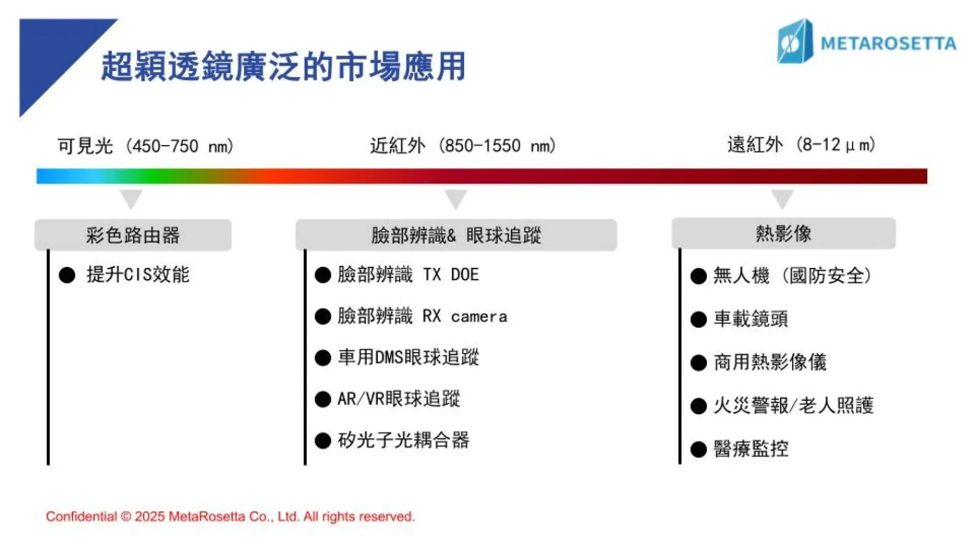
Currently, meta-lens technology is mainly being developed in two major infrared light application scenarios:
The first is near-infrared (NIR) applications, encompassing high-precision sensing technologies such as facial recognition and eye tracking, which are widely used in mobile phones and wearable devices. Consumer electronics brands, represented by Apple, are also actively adopting related technologies to reduce module size and improve sensing performance.
The second application is far-infrared (LWIR), primarily used for thermal imaging sensing, with applications in industrial inspection, security monitoring, and defense. This type of technology was previously limited by material costs and size, but with the development of metalenses, new possibilities are gradually being unlocked.
Despite its enormous potential, the key reason why meta-lenses have been difficult to put into practical use in the past is the gap between cost and "design and manufacturing process".
A key breakthrough in enabling the mass production of optical designs
Optical design and semiconductor manufacturing processes are essentially two distinct fields: one relies on the principles of optical refraction, while the other is built upon wafer miniaturization and etching processes. Integrating the two has long been a challenging problem for the industry.
MetaRosetta's solution is to create an AI optical design platform called "Meta Rosetta".
This system first solves the problem of "disconnect between design and mass production" in actual manufacturing processes. In the past, nanostructure designs mostly remained in the theoretical or laboratory stage. Once they entered the wafer fab, they were often unable to be produced or had extremely low yields because the structures were too small or the arrangements were too complex, exceeding the etching limits of semiconductor equipment.
To address this, MetaRosetta employs a "process-oriented design" approach, incorporating manufacturing constraints from the initial design phase. The system features process screening and error-proofing mechanisms, automatically filtering out structures that do not meet foundry requirements. Combined with AI optimization algorithms and GPU-accelerated computing, the design process, which originally took months, is compressed to within tens of minutes, and product yield can be predicted, ensuring that the design results can be successfully mass-produced.
In addition to the design itself, Koinda also overcame the data challenges brought about by large-aperture meta lenses.
When the size of a meta-lens increases to the 2-centimeter level, its surface has tens of millions of nanostructures that generate extremely large photomask files, making it difficult for design software to process and even impossible for factory equipment to read.
To address this pain point, Koinda developed a unique compression algorithm that reduces the size of the photomask file by up to 1,000 times, allowing the design to seamlessly integrate with the wafer fab production process. This is one of the keys to their ability to produce large-aperture thermal imaging super lenses.
From the research lab to the global supply chain: a proven track record of commercial success.
Currently,MetaRosetta has achieved substantial results in both major application areas (near-infrared and far-infrared).
In the near-infrared field, through in-depth cooperation with the supply chain, we have entered the global consumer electronics brand system and participated in the design of key optical components for major Japanese manufacturers.
In the far-infrared field, they launched the world's first 2 cm large-aperture thermal imaging super lens, and won the 2025 CES US Army x Tech competition with this achievement, attracting the attention of the US defense industry.
These impressive international achievements are no accident; they are backed by a cross-disciplinary team with profound optical knowledge and practical experience in semiconductors.
MetaRosetta's CEO, Hsu Wei-lun, holds a Ph.D. in Physics from National Taiwan University and had extensive experience in the semiconductor industry before the company's official establishment in 2025. His team members span semiconductor manufacturing, packaging, and academic research, bringing together experts from UMC, Samsung, Compal, and Academia Sinica, who have a deep understanding of the gap between traditional optical design and semiconductor manufacturing.
Recalling how they started their business, Dr. Hsu Ying-hsin (pictured), the current Executive Vice President, mentioned that the two met as early as 2019. At that time, she was working as a startup mentor in southern Taiwan, and Hsu Wei-lun contacted her as a consultant to explore the feasibility of using optical technology in sensing devices. Although they had not officially formed a team at that time, the two had already formed a bond since then.
It wasn't until 2023 that Hsu Wei-lun invited her again with mature technology developed in collaboration with a research team at National Central University. He frankly stated that the team consisted entirely of PhDs in physics and optics with technical backgrounds and that they desperately needed talent with business and finance experience. Only then did Hsu Ying-hsin officially join the team.
After the team was formed, it immediately joined the National Science Council's "Scientific Research and Entrepreneurship Program". Within just one year, it completed the stress test from academic research to commercialization verification and gradually began to gain exposure and recognition in major international exhibitions and competitions.
The development of super-lenses may be similar to the evolution of 5G and Wi-Fi technologies. At first, the public may not be able to perceive the difference, but looking back a few years later, they will find that the convenience they bring has completely changed their lives.
MetaRosetta is trying to secure a key position in this "invisible" technological revolution and continue to cultivate the US and Japanese markets, so that Taiwan's technological strength can have a greater influence on the international stage.