
MetaRosetta enters the photon generation TREE market to help it expand its presence in the US.
2026.06.03
Article quoted from:https://strategicstyle.org/s-market-8374/24923/
Starting with super-sensitive lenses, the development is moving towards photonics and optoelectronics.
Driven by the rapid development of AI and HPC, the global technology industry is transitioning from electronic computing to the era of photonics technology. From machine vision to data center transmission, "light" is gradually becoming the core of the next generation of computing and sensing. However, the limitations of traditional optical systems in terms of size, efficiency, and integration have become major bottlenecks for industrial upgrading.
MetaRosetta has announced its selection as a team member for the Ministry of Economic Affairs' TREE International Linkage and Proof-of-Concept Landing Program, marking the start of its expansion into the Americas market. Starting with Metalens, MetaRosetta will leverage its self-developed optical design platform to gradually build cross-scale light field control capabilities, further extending into the fields of silicon photonics and optoelectronic integration.
A self-developed optical design system could enable mass production.
Dr. Hsu Wei-lun, CEO of the MetaRosetta team, pointed out that most metasurface technologies are still in the academic and single-component development stage, making it difficult to enter mass production and system integration. However, the real challenge is not the physical limits, but the gap between design and manufacturing.
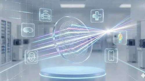
To address this challenge, MetaRosetta built its own optical design system, combining semiconductor process limitations with design for manufacturing optimization, enabling the mass production of super-intelligent lenses at the wafer level. This system allows for highly flexible design of the optical field and phase for different wavelengths of visible light, near-infrared to long-wave infrared, transforming the company from a single optical component designer into a technology provider with "system-level optical design capabilities."
Image sensing drives composite super lens design
MetaRosetta points out that in the field of image sensing, it has launched a "composite super-lens" design. Through the synergistic optimization of multi-layer optical structures, it can effectively correct aberrations and improve image quality, and still achieve high-resolution images under miniaturization conditions.
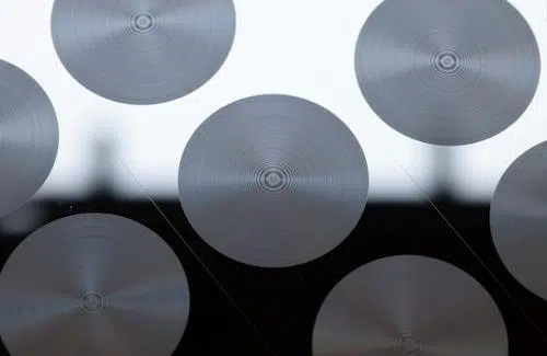
This technology has already been applied to thermal imaging fields. After winning the US military's Xtech Finnal Winner award at the CEO event last year, the team's technology has now entered the verification process of specific defense customers, demonstrating its potential in high-reliability application environments. Such miniaturized, high-performance optical modules can be widely used in drones, autonomous driving, defense and industrial inspection in the future.
System-level optics optimizers advocate for optoelectronic co-design.
In the fields of optical communication and high-performance computing, silicon photonics technology is considered key to overcoming data transmission bottlenecks. However, problems such as off-axis dispersion, mode mismatch, and energy loss still exist in the optical coupling process between the chip and the environment, limiting the overall system performance.
MetaRosetta points out that by utilizing the high degree of freedom in phase design capabilities of super-lenses, precise control of the light field can be achieved, which can effectively improve optical coupling efficiency and mode matching and reduce system losses. Positioning itself as a "system-level optical optimizer", it assists semiconductor and system manufacturers in improving the overall performance of existing silicon photonics platforms and promotes the development of optoelectronic co-design.
Constructing a complete solution for bridging semiconductor photonics technology
With its selection for the US Landing Program this year,MetaRosetta is actively expanding into the Americas market, targeting key supply chains such as defense and aerospace, autonomous driving, and high-performance computing. The MetaRosetta team stated that, leveraging its military-grade verification experience with thermal imaging products and its silicon photonics design capabilities, it has the opportunity to further penetrate the "trusted supply chain" system, providing next-generation optical key components and design services.
Currently, MetaRosetta is working with domestic and international semiconductor foundry partners to integrate manufacturing processes and is accelerating the development of 8-12 inch wafer-level mass production capabilities. Hsu Wei-lun emphasized that in the future, Koinda will not only provide individual optical components but will also strive to build complete solutions from design and manufacturing to system integration, becoming a key bridge connecting semiconductor and photonics technologies. With the continued convergence of AI sensing and photonic computing,MetaRosetta aims to define the next generation of optoelectronic integration technology standards based on its advanced optics.